Meeting the Rising Demands of a Rapidly Evolving Semiconductor Industry
Today’s devices must perform under tighter thermal envelopes, smaller footprints, and faster cycle times, all while staying aligned with the demands of next-gen applications, like automotive autonomy or edge AI. Test systems can no longer just confirm functionality. They must measure near the limits of timing, and keep up with shifts in materials like SiC, GaN, and MEMS.
Where Semiconductor Testing Gets More Complex
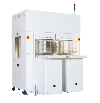
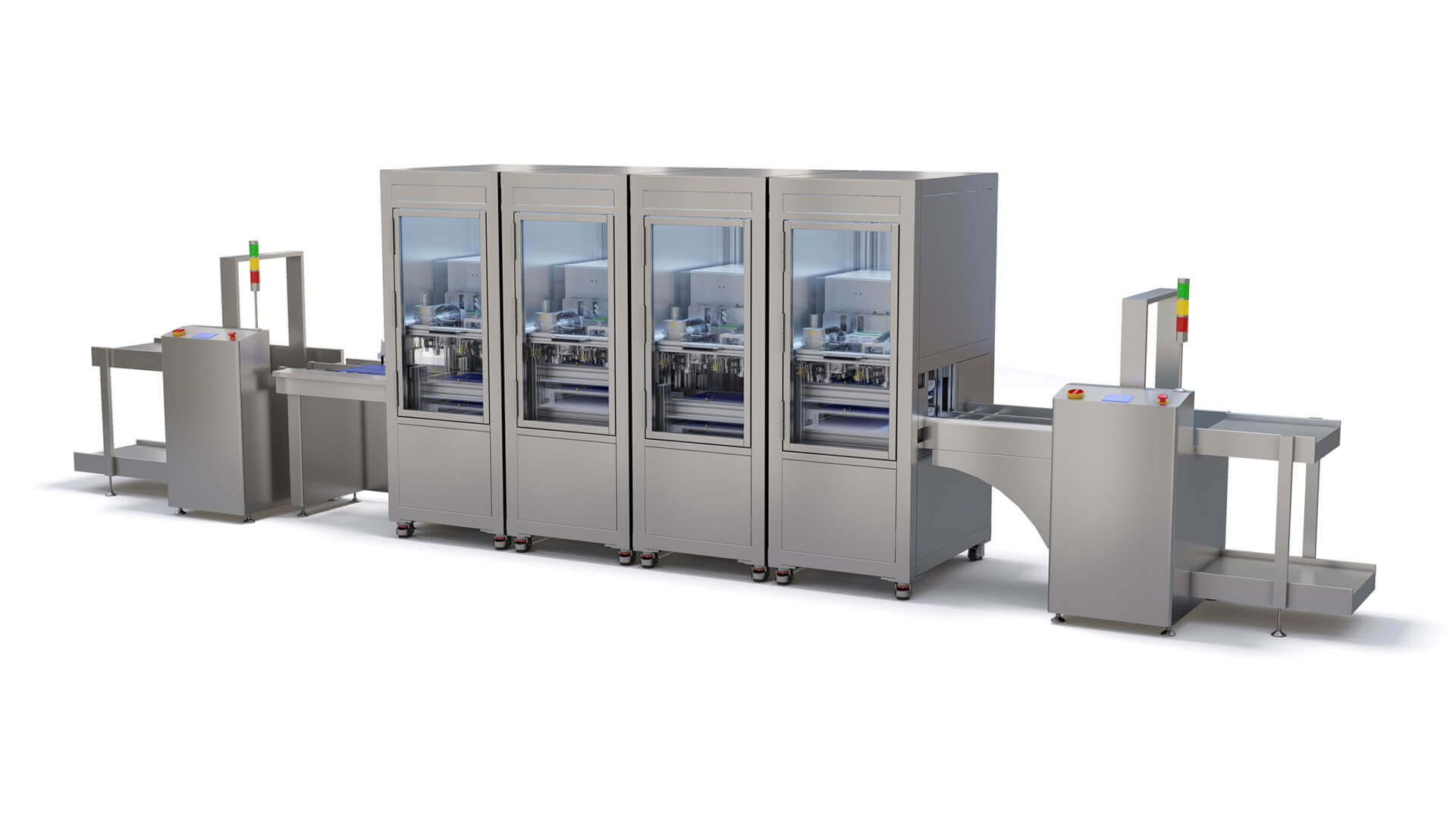
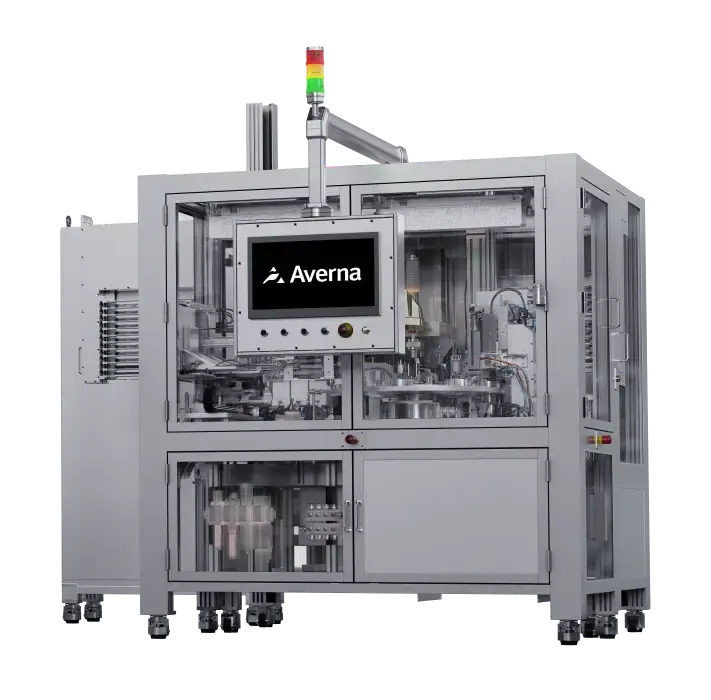
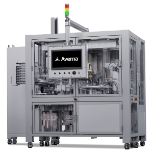
The semiconductor industry requires multi-domain test environments. Electrical and mechanical handling, optical inspection, protocol verification, all now interact within the same flow. Challenges arise from:
- Maintaining sub-micron alignment in wafer handling while scaling throughput
- Capturing transient electrical or optical behavior under environmental stress
- Generating test coverage for MEMS, ASICs, or multi-chip modules with stimulus simulation
- Meeting SEMI S2/S8/S22 requirements while optimizing cleanroom compatibility
These challenges require tailored systems, domain-specific expertise. That’s only by partnering with an engineering partner who speaks the language of modern fabs you can achieve this.
Averna’s Technical Expertise Across Semiconductor Applications
Averna delivers modular and automated test systems tailored to semiconductor production. Our platforms support critical processes such as wafer-level sorting, package testing, burn-in, I-V and C-V characterization, as well as in-system functional validation.
We engineer test environments capable of simulating real-world conditions, enabling traceable, repeatable testing across diverse wafer sizes and operating thresholds. Whether the goal is to accelerate time to market or ensure fault-proof integration, our systems meet the requirements of modern fabs and regulatory bodies alike.
These capabilities are vital across industries such as automotive, aerospace, consumer electronics, medical devices, industrial automation, and telecommunications, where chip reliability and system integration are non-negotiable.
Key Areas of Expertise
Our solutions are tuned for technical precision and cleanroom compliance, addressing a wide range of semiconductor challenges:
- Wafer and die-level testing, with integrated burn-in environments and electro-optical inspection tools
- MEMS characterization, including motion, pressure, acoustics, light, humidity, and magnetism, with physical stimulus integration
- Generating test coverage for MEMS, ASICs, or multi-chip modules with stimulus simulation
- IC, ASIC, and SoC full-cycle verification, with parametric analysis under temperature variation
- Inline vision inspection, from PCBA solder joints to micro-assembly quality gates
- Risk and standards validation, including SEMI S2/S8/S22 documentation and CE/IEC readiness
- Final test stations, optimized for analog, mixed-signal, and high-speed digital components
Averna’s Semiconductor Test Equipment
|
|
|
|
EFEM Wafer Handling PlatformUltra-clean automated wafer handling platform with FOUP/SMIF interface options, precision wafer alignment, and seamless robotic integration.
|
Uniline for Mixed Functional & EOL TestingScalable station for electrical, ICT, safety, and functional test coverage with full automation, ideal for ASIC modules and PCBA assemblies. |
Active Alignment Assembly & Test PlatformSee how our industry established platform can accelerate production and improve product quality. Ideal for manufacturers seeking repeatable precision assembly services at scale.
|
Vision Inspection SystemsOptical systems optimized for micron defect detection, bond inspection, solder paste validation, and final product classification.
|
Work with Averna to Accelerate Your Semiconductor Testing Roadmap
From smartphones and wearables to automotive and aircraft – talk to our test and quality experts about our MEMS, product characterization and validation test solutions.
Learn More About our Semiconductors Advanced Test and Measurement Solutions
Success Story
Learn how we implemented an extremely precise and 100% accurate Vision System that dramatically improved their PCB printing results.
Contact our semiconductor testing team today
Accelerate your time to market with our proven semiconductor test solutions. We’re just a message away: reach out today!


