Support
    • Smart ManufacturingSmart manufacturing solutions that connect test systems, data, and automation to enable real-time visibility and predictive insights.
    • Prototyping & ConsultingEarly-stage Design for Testability (DFT) analysis, flexible prototyping, and proof-of-concept validation.
    • Automated Test Solutions (ATE)High-speed benchtop and cabinet-level verification, validation and testing.
    • In-Line Test SystemsContinuous conveyor line automated test or inspection with zero-cycle interruption.
    • Precision Assembly & ProductionAutomated assembly solutions with advanced robotics, inspection, and process control for zero-defect manufacturing.
    • Test System ReplicationGlobal multi-site deployment of identical test systems with obsolescence control.

    Bring Your Quality to the Next Level.

    Explore scalable quality solutions engineered for the world’s most demanding high-reliability products and automated manufacturing environments.

    Talk to an expert
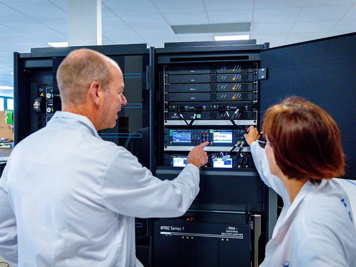
    Engineers manipulating an ATEC ATMOS test station

    Our flexible test platforms are built on proven architectures with integrated IP, enabling maximum reuse and faster deployment for product design, manufacturing and support.

    Find the right platform for your application
    Explore all RF instruments
    Explore all software solutions
    Knowledge & Engineering

    Visit our Resource Center for videos, white papers, brochures & eBooks

    Resource Center
    • About usAverna Powered by Spherea is recognized as a worldwide Test & Quality Engineering leader, delivering innovative, end-to-end solutions that accelerate time-to-market and ensure flawless performance.
    • Technology PartnersTo ensure we provide the best possible solutions and integration services to our customers, we are strategically aligned with the world’s top test and technology companies.
    • ESG & SustainabilityWe are more committed than ever to honor our role as an employer, supplier, and customer by contributing positively to our communities.
    • CareersJoin our team full of incredible talent and inspire the future of test. Our people are who make us who we are and we demonstrate this through our values everyday!

    Bring Test to the Next Level

    Our team of 1800 specialists are passionate about delivering engineering innovation, zero-defect quality architectures, and mission-critical automated testing systems across the product lifecycle.

    60+ YearsTest Experience
    20,000+Completed Projects
    Download our Corporate Profile
    EFEM Platform

    Our EFEM Platform offers ultra-clean, reliable performance for wafer handling.


    One to four+ FOUP or SMIF interfaces.


    High-precision wafer alignment capabilities and wafer flip option.


    3- and 4- axis robots available as a standard design.


    Mini-environment for contamination control as well as airborne molecular contamination filter options.


    Optimized for cost and contamination levels to meet ISO-class cleanroom needs.


    300, 200, 150 and 100 mm circular wafers (customizable to other materials, shapes and sizes).


    Adaptable to different wafer technologies including film-frame carrier strategies, taiko wafers, thin/thick wafers, bonded wafers, non-flat wafers or wafers with 3D structures, and glass wafers.

    A Complete Solution for Optimal Results

    Our EFEM Platform can act as a standard EFEM, or can be customized to suit your application’s cleanliness, handling technique, throughput, and form-factor requirements. From design to manufacturing, we offer units in varying complexity and precision and can integrate the needed hardware, software, vision, optics design, sub-micron metrology, environmental control and materials handling to fit your needs from single units to 4-wide.

    Get to Market Faster

    By having all the capabilities you need under one roof, delivering flawless products is significantly simplified. Our options include: 

    • A range of end effector technologies: Bernoulli, edge grip, or vacuum grip
    • ESD charge control options
    • Vacuum and low contamination integration capabilities
    • Configurable layout for process simplification and/or footprint/form factor optimization
    • High accuracy aligner systems to 10 µm accuracy
    • Experience with integrated vibration isolation

      CONTACT US

    Additional Features: Vision, Optical and A.I. Expertise

    Additionally, we offer optical and vision system design capabilities including barcode readers, optical character recognition (OCR), defect analysis and characterization, contamination detection and flatness measurement. Integration of additional sensor technology can be offered, as required. Our in-house predictive reliability analysis software allows for continuous system monitoring and response.

    Safety, Reliability and SEMI Compliance

    Our EFEM is a reliable platform with a high MTBF and solid performance. It meets CE and SEMI standards for hardware and software including S2, S8, E84, E87, E58.

    Customization Options and Features: 


    EFEM Platform

    Environmental

    • Mini-Environment for up to ISO Class 1 Operation
    • Temperature Control
    • Electrostatic Charge Reduction
    Wafer Handling
    • Wafer Size: 300, 200, 150, 100
    • Accommodates Various Thicknesses and Warped Wafers
    • Varying Substrate Materials (Glass, Silicon, Silicon Carbide, Germanium)
    • End Effectors or Various Gripping Technologies (Edge, Vacuum, Bernoulli)
    • Wafer Flipping
    • Special Wafers or Other Substrates (Reticles, Film Frame, Display, JEDEC Trays)
    • Industry Standard SMIF and FOUP Load Ports
    • Accommodates Special Modules such as High-Precision Aligners
    Robotics
    • Single and Dual Arm
    • 3-Axis and 4-Axis

    Vision & Optical

    • Barcode Readers
    • Fiducial Recognition
    • OCR
    • Defect Analysis and Characterization
    • Flatness Analysis
    Software Requirements & Features
    • Standard 300 mm & 200 mm SEMI Compliant Libraries
    • Interfacing Protocols to Host Controller in Standard EFEM
    • SMEMA & SECS/GEM Interfaces
    • Data Management and Tracking Capabilities
    • SEMI E95 Compliance for Human Machine Interface (HMI)
    • Wafer Mapping