Support
    • Smart ManufacturingSmart manufacturing solutions that connect test systems, data, and automation to enable real-time visibility and predictive insights.
    • Prototyping & ConsultingEarly-stage Design for Testability (DFT) analysis, flexible prototyping, and proof-of-concept validation.
    • Automated Test Solutions (ATE)High-speed benchtop and cabinet-level verification, validation and testing.
    • In-Line Test SystemsContinuous conveyor line automated test or inspection with zero-cycle interruption.
    • Precision Assembly & ProductionAutomated assembly solutions with advanced robotics, inspection, and process control for zero-defect manufacturing.
    • Test System ReplicationGlobal multi-site deployment of identical test systems with obsolescence control.

    Bring Your Quality to the Next Level.

    Explore scalable quality solutions engineered for the world’s most demanding high-reliability products and automated manufacturing environments.

    Talk to an expert
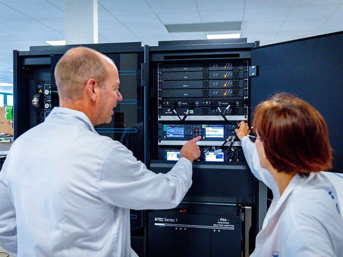
    Engineers manipulating an ATEC ATMOS test station

    Our flexible test platforms are built on proven architectures with integrated IP, enabling maximum reuse and faster deployment for product design, manufacturing and support.

    Find the right platform for your application
    Explore all RF instruments
    Explore all software solutions
    Knowledge & Engineering

    Visit our Resource Center for videos, white papers, brochures & eBooks

    Resource Center
    • About usAverna Powered by Spherea is recognized as a worldwide Test & Quality Engineering leader, delivering innovative, end-to-end solutions that accelerate time-to-market and ensure flawless performance.
    • Technology PartnersTo ensure we provide the best possible solutions and integration services to our customers, we are strategically aligned with the world’s top test and technology companies.
    • ESG & SustainabilityWe are more committed than ever to honor our role as an employer, supplier, and customer by contributing positively to our communities.
    • CareersJoin our team full of incredible talent and inspire the future of test. Our people are who make us who we are and we demonstrate this through our values everyday!

    Bring Test to the Next Level

    Our team of 1800 specialists are passionate about delivering engineering innovation, zero-defect quality architectures, and mission-critical automated testing systems across the product lifecycle.

    60+ YearsTest Experience
    20,000+Completed Projects
    Download our Corporate Profile

    MEMS Device Testing Built for High-Volume Quality Control

    microchip-mems-testingAccurate, low-cost quality control is key when MEMS devices ship in high volumes, and each part still needs individual validation and characterization. Most of that cost sits at final test, where physical stimulus is required to prove each function.

    Averna Powered by Spherea designs test systems that combine physical stimulus with micron-level probing in one automated cell, so every MEMS device is characterized at production speed. 

    How Averna Approaches MEMS Testing

    There is no need to wait for volume production. Averna steps in wherever a MEMS program needs test support, whether that means characterizing a first prototype or equipping a production line. 

    1. Phase 01

      Define the test strategy

      Engineers map each device function to the stimulus and measurement it requires, then set pass/fail limits with the design team.
    2. Phase 02

      Characterize in R&D

      Semi-automated probing and resonant characterization validate new designs before volume, with results fed back to engineering.
    3. Phase 03

      Screen at wafer probe

      Fine-pitch probing rejects defective dies before packaging, so packaging spend goes only to good parts.
    4. Phase 04

      Validate at final test

      Averna’s automated test solutions apply physical stimulus under controlled temperature and sort each packaged device by result.
    5. Phase 05

      Consolidate test data

      Results from every stage feed a single data flow for traceability and yield analysis.

    Applications Across MEMS Markets

    Microelectromechanical systems (MEMS) devices need to be tested in various industries.

    Icon - Semiconductor Artboard

    Semiconductor MEMS Production

    Wafer probe testing and package-level semiconductor testing for inertial and pressure sensors in high-volume fabs.

    Icon - Telecom Infrastructure

    Telecom and Optical Networks

    Insertion loss and switching repeatability checks for MEMS-based optical devices in next-generation networks.

    Icon - Automotive (EV)

    Automotive Sensors

    Tri-temperature validation that builds MEMS reliability data for ADAS and vehicle stability sensors.

    Icon - Consumer Electronics

    Consumer Electronics

    Acoustic and motion characterization for MEMS microphones and IMUs in smartphones and wearables.

    Icone-Aerospace and Def

    Aerospace and Defense

    Environmental stress and mechanical cycling for inertial MEMS used in flight and guidance systems.

    Icon - Life sciences

    Life Sciences and Medical Devices

    Pressure sensor characterization for medical devices, run under cleanroom conditions that protect measurement accuracy.

    Looking for MEMS Testing Equipment?

    Moving a MEMS design toward volume production? Talk to Averna engineers about the right test approach.

    Contact us

    Technical Capabilities for MEMS Testing

    Every Averna MEMS test system is designed for a specific device, so modularity is built in from the start. The capabilities below are combined to match the package and production volume of each program.

    Fine-Pitch MEMS Wafer Probe Testing

    Averna probing systems move multiple probes independently in X, Y and Z, reaching probing accuracy below 3 µm. Vision algorithms align probe needles to a wide variety of pad patterns. Handling accepts wafers or packaged devices, and robotized loading supports fully automated MEMS micro-probing.

    Physical Stimulus and Resonant Characterization

    A MEMS response only means something when it is tied to a real physical input. Averna integrates stimulus for motion, pressure, light, humidity and magnetism directly into the test cell. Parallel acquisition runs resonant characterization across many channels at once, while high-speed digitizers capture transient behavior during R&D.

    MEMS Microphone Testing

    Microphones need a controlled acoustic field and isolation from ambient noise. Averna builds acoustic stimulus into the test cell, so sensitivity and frequency response are measured on each device during production.

    Thermal Conditioning and MEMS Reliability

    Tri-temperature conditioning reproduces the operating extremes of automotive and aerospace environments. Thermal performance parameters are tracked precisely throughout each cycle. Mechanical cycling and environmental stress testing complete the picture, generating the MEMS reliability data programs need before release.

    Optical MEMS and Active Alignment

    For MEMS-based optical devices, Averna validates motion and position accuracy alongside electrical response. Optical switch testing covers insertion loss, return loss and cross-talk under repeated switching. Active alignment of fiber array units to photonic integrated circuits brings MEMS precision assembly and testing into a single precision process.

    High-Throughput MEMS Testing Equipment

    Soft-impact pick and place handles packages as small as 1 x 1 mm, including flex foils. Input and output adapt to tray, bowl feeder, wafer or tape and reel, and conversion kits support standard and custom packages. Laminar airflow keeps the test zone at ISO 14644-1 Class 5. As an NI Diamond Partner, Averna Powered by Spherea develops test software in LabVIEW and TestStand on PXI-based architectures, which shortens application development.

    Proven MEMS Test Capabilities

    The figures below come from MEMS test systems Averna has already designed and built. They show the level of precision the engineering team brings to every new project. 

    Technical Specifications

    Capability Demonstrated Performance
    Probing accuracy < 3 µm, with independent X, Y and Z motion per probe
    Probe geometry 100 µm pitch, 5 µm tip size
    Contact density 64 needles per probing cycle
    Parallel resonant characterization

    64 channels simultaneously at 400 MB/s

    High-speed resonant characterization 2 GS/s sampling
    Thermal conditioning -40 °C to 150 °C, ±1 °C accuracy
    Device handling Packages down to 1 x 1 mm, leaded, leadless or flex
    Input and output formats Tray, bowl feeder or wafer input; tray, tape and reel or bulk output
    Test environment ISO 14644-1 Class 5 laminar airflow
    Integrated vision Needle-to-pad alignment, 2D/3D optical inspection, OCR and dot matrix code reading

    Start Your MEMS Testing Project

    Bring your MEMS device to Averna Powered by Spherea and leave with a test strategy ready for production.